Product Manager, Brooks Automation
A batch of printed circuit boards (PCBs) leaves the factory with solder joints that looked ok but contained hidden voids, micro-cracks, and head-in-pillow joints. Standard inspection didn’t catch the issues, and once installed in the customer’s product, the boards began failing within days.
Suddenly, the manufacturer is faced with warranty claims, product returns, and the possibility of a costly recall. For test and manufacturing engineers, this is the nightmare scenario PCB testing is meant to prevent.
That’s why methods like in-circuit testing, functional testing, burn-in, and electrical safety checks are essential to prove every board is reliable before it ships. But in high-mix production, where lots are smaller and changeovers are constant, manual test loading becomes the weak point. Robotics removes this bottleneck, keeping testing consistent, traceable, and scalable.
8 PCB Testing Methods That Ensure Reliability and Compliance
Before looking into individual approaches, it helps to see PCB testing as a layered process.
Different tests address different risks: some check that the bare board was built correctly, others confirm the assembly is sound. The most important ones prove the board works properly in real-world conditions and meets standards. Used together, they create overlapping safeguards that reduce the chance of defects escaping into the field.
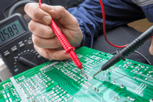
1. Bed-of-nails in-circuit testing (ICT)
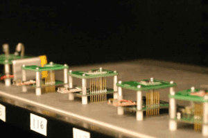
Source: Hillman Curtis
In-circuit testing is one of the most established methods for verifying PCB assembly quality. It relies on a custom “bed-of-nails” fixture, where hundreds or even thousands of spring-loaded test pins simultaneously press against designated nodes on the board. This setup enables rapid, repeatable measurements of electrical parameters such as shorts, opens, component values, and part orientation.
ICT is often described as having 100% theoretical coverage, since every accessible node can be probed. In practice, dense layouts, hidden pads, and complex packages limit achievable coverage to around 85–90%.
The method is highly effective at catching assembly-level defects early, but it also demands careful design-for-test planning during the PCB layout phase.
Each new board design requires its own fixture, which represents a significant upfront investment in both cost and lead time. Even with these drawbacks, ICT is still widely used in high-volume electronics manufacturing because it is fast, accurate, and well-suited for testing large batches of boards.
2. Functional Testing
Functional testing verifies that a finished PCB performs as intended when powered under realistic operating conditions. Unlike inspection methods that focus on structure or component presence, this test exercises the board’s circuitry through its actual inputs and outputs, firmware, and timing responses.
The scope can vary widely:
- Simple power-on and boot sequence check (for some products)
- Comprehensive scenario testing with:
- Custom test fixtures
- Software scripts
- Simulated peripheral devices
Because functional testing evaluates how the board interacts with its environment, it often uncovers issues that earlier structural or parametric tests miss. Issues such as firmware misconfiguration, intermittent connections, or timing margins that fail under load.
3. Burn-in and environmental stress testing
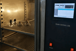
Burn-in subjects boards to elevated electrical loads and higher-than-normal operating temperatures for an extended period of time. The goal is to accelerate latent defects. It forces early-life component or solder joint failures to appear before shipment. In practice, boards may be powered continuously or cycled on and off while held in temperature-controlled chambers. These conditions mimic years of field operation in just a few days.
Typical durations in manufacturing range from 48 to 168 hours. Though the exact profile depends on product requirements, reliability targets, and the risk tolerance of the manufacturer. Some programs combine burn-in with vibration or humidity exposure to further uncover weaknesses in assembly quality or component robustness.
4. Flying Probe Testing
Flying probe uses programmable test pins (probes) that move to test different points on the PCB without a custom fixture. It adapts quickly to new PCB designs, which makes it ideal for prototypes and high-mix or low-volume work. The trade-off is speed, since the probes must move to each test point. This motion limits throughput compared to fixture-based systems.
5. Automated Optical Inspection (AOI)
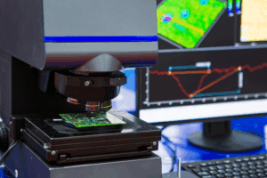
AOI uses 2D or 3D imaging to compare the assembly against golden data—a reference model of a defect-free board. It flags issues such as solder bridges, missing or misaligned parts, and mask defects.
Because AOI is non-powered and does not cover all components, it is generally paired with an electrical method such as ICT, flying probe, or functional test.
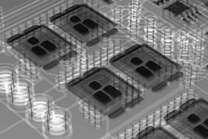
6. Automated X-ray inspection (AXI)
Source: Kuttig Electronic
Automated X-ray inspection (AXI) reveals hidden features that cannot be seen with optical methods. These include:
- BGA balls: the solder balls underneath ball grid array (BGA) packages that connect the chip to the PCB.
- Internal vias: plated holes inside the board that provide electrical connections between layers.
- Barrel fill: the completeness of solder filling inside a plated through-hole via.
AXI is used for dense surface-mount technology (SMT) assemblies, where components are mounted directly on the board surface and joints are hidden under packages.
Interpreting X-ray images requires trained operators. Defects such as voids or incomplete solder joints can be subtle and misinterpretation could lead to false passes or unnecessary rework. The process also adds cost and time compared to optical inspection.
7. Electrical impedance testing
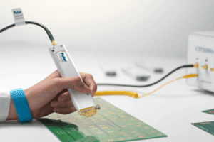
Source: Polar Instruments
High-speed PCBs need carefully controlled impedance. If impedance is not consistent along a trace, signals can reflect or distort, reducing reliability.
To check this, manufacturers use time-domain reflectometry (TDR). This method sends a pulse through a test coupon (a small piece of the PCB made for measurement) or a fixture. Any discontinuities or changes in impedance caused by poor etching, plating, or layer alignment are revealed in the reflected signal.
The industry standard IPC TM-650 provides detailed procedures for measuring characteristic impedance and signal loss.
If your design includes high-speed interfaces such as USB, HDMI, or DDR memory, impedance testing is essential to ensure your PCB will work as intended in real-world conditions.
8. Bare-board electrical tests
Before components are added, fabricators run bare-board electrical tests to check the copper integrity of the PCB. These tests confirm that all traces, vias, and layers conduct properly without opens or shorts.
These checks are compared against the design netlist, which is the circuit connectivity map generated from the CAD design.
The standard IPC-9252B defines how to perform these continuity and isolation tests, both with direct probing and indirect methods.
In practice, most fabricators test 100% of bare boards to this standard to confirm the stack-up is correct before assembly begins.
Other functional and quality tests
Depending on the product, additional tests include:
- Solderability testing to confirm wetting and joint reliability.
- Ionic cleanliness assessments, such as ROSE or SIR to control corrosion risk.
- Micro-section analysis to inspect internal structure and plated through holes.
- Peel and solder-float tests for laminate adhesion and thermal stress capability.
Electrical Safety Tests for PCB Compliance
Beyond proving functionality, PCBs must also pass safety checks that verify they will not create shock, fire, or grounding risks in the field. They are especially important in sectors where failures can pose risks to users or prevent certification, such as automotive, medical devices, and consumer electronics. IPC, UL, IEC, and ANSI/ESD S20.20 all reference these procedures, making them an expected step when compliance is required.
- Dielectric withstand (hipot) testing: Applies high voltage between isolated circuits to confirm insulation integrity.
- Insulation resistance testing: Measures resistance between conductors to ensure it exceeds safety thresholds.
- Leakage current testing: Quantifies unintended current flow through insulation or across surfaces under voltage.
- Ground bond testing: Verifies that protective grounding paths are secure and effective.
These tests are often run near the end of the production cycle, providing documented evidence that boards are safe and meet regulatory requirements before shipment. For manufacturers serving regulated markets, passing them is essential for compliance, customer trust, and long-term reliability.
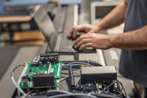
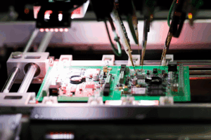
Manual Test Loading Bottlenecks to Robotic Solutions
PCB test methods such as ICT, functional testing, and burn-in are highly effective. However, the way boards are loaded into fixtures and racks often determines whether those tests deliver consistent results. Manual handling can misalign boards in fixtures, stress connectors, or introduce ESD risk. In high-mix environments, where changeovers are frequent, these inconsistencies reduce test reliability.
This is where automation makes the difference. Beyond catching defects, robotics addresses three persistent challenges in PCB testing:
- Unpredictable Throughput: Operators switching between SKUs and fixtures create cycle time variability. Robotics standardizes the process: every board is placed the same way, every cycle runs at the same pace, and fixture changeovers are handled by programmed routines. This makes throughput steady even as product variety increases.
- Labor Limits in High-Mix Testing: Training operators for precise, repetitive tasks is resource-intensive, and fatigue or turnover affects consistency. Robots expand testing capacity without additional headcount, enabling continuous operation in labor-constrained environments.
- Traceability and Data Integrity: Manual serialization and data entry can create gaps in MES records. Robots scan barcodes automatically and link every test to a unique board ID, giving manufacturers complete and auditable traceability.
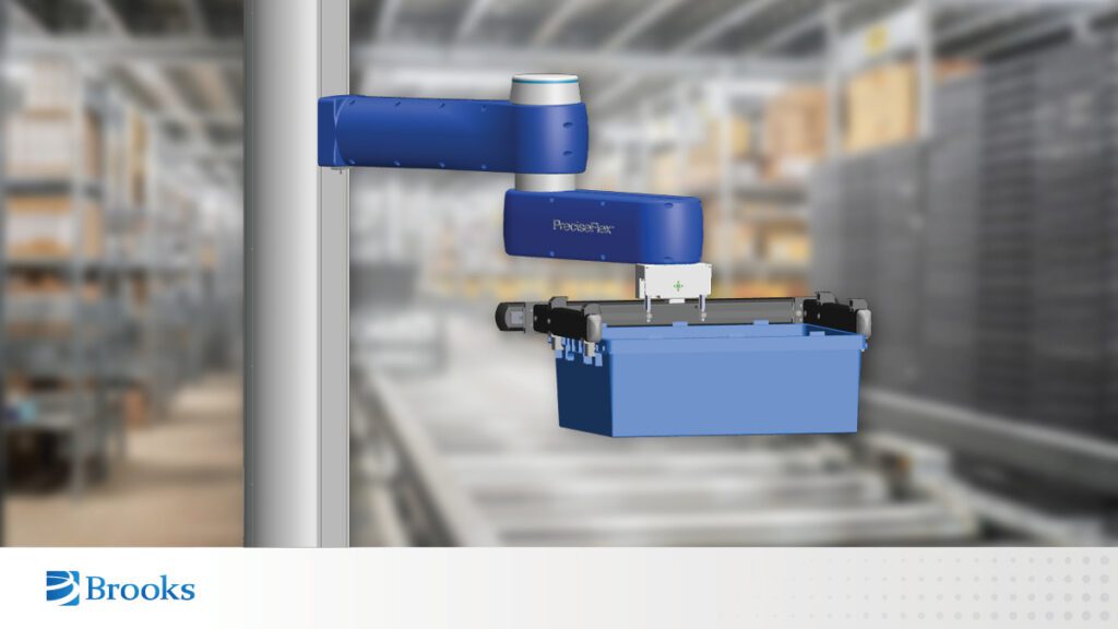
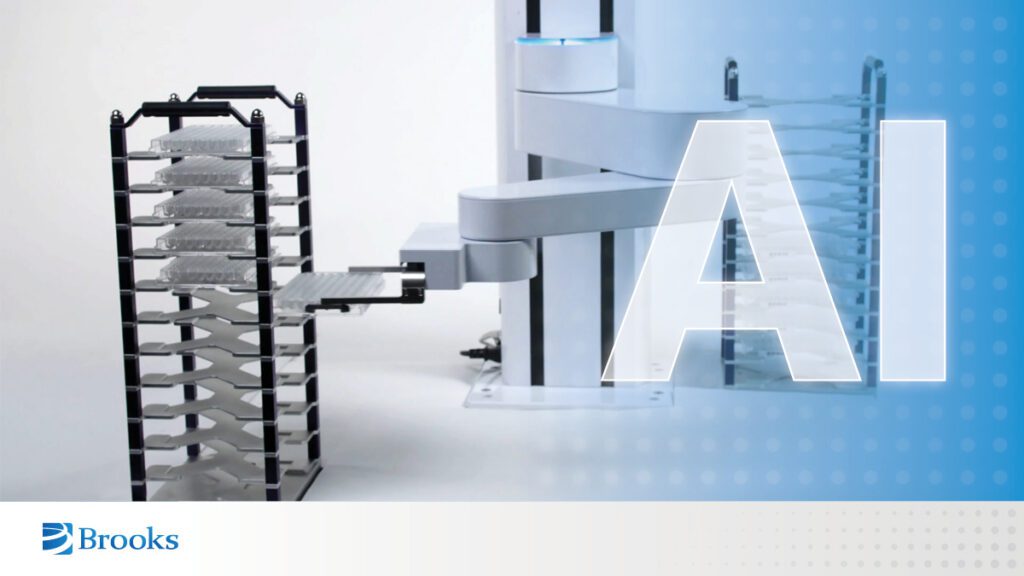
PreciseFlex Robots Fit
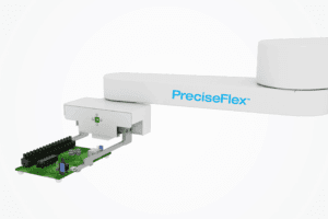
Brooks PreciseFlex robots are purpose-built to handle PCBs reliably during testing. Rather than managing entire test setups, they place boards into in-circuit test fixtures, seat them for functional testing, and load or unload them into burn-in racks. The same precise, repeatable motions are also used for tasks such as moving boards to flash programming stations or transferring assemblies between production machines.
With vision-enabled grippers and controlled force, the robots ensure proper alignment without stressing connectors or components.
PreciseFlex robots are compact enough to fit into crowded test cells, need little maintenance, and are collaborative by design, allowing them to operate safely alongside people.
For many electronics manufacturers, PreciseFlex has already demonstrated consistent productivity and return on investment in under a year, even in small and midsize facilities.
Get the Electronics Test whitepaper for real-world case studies, cost comparisons, and step-by-step implementation insights.
Download the Electronics Test Whitepaper
Optimize PCB Testing with PreciseFlex Robots
PCB testing methods are vital for ensuring boards leave the factory free of defects. In high-mix production, the tests themselves are only as effective as the process that supports them.
Manual handling like loading fixtures, engaging connectors, and tracking serialization, slows throughput and introduces variability. Streamlining these steps with automation makes proven test methods more consistent and efficient. Robotic test handling delivers steady cycle times and complete traceability through MES integration.
With compact footprints, embedded controls, and vision-enabled grippers, PreciseFlex robots fit easily into ICT, functional, and burn-in cells. Safe to operate alongside people and proven to deliver ROI in under a year, PreciseFlex robots make scaling PCB testing practical for both small and midsize facilities.