
Product Manager, Brooks Automation
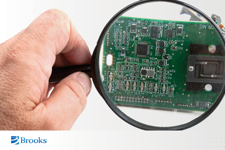
Every PCB that leaves the line carries your reputation with it. If a defect slips through, the result is almost always the same: rework, lost time, and an unhappy customer.
Inspection reduces that risk, but keeping up with demand is the challenge. Yields need to improve, cycle times keep shrinking, and it’s not practical to solve the problem by adding more people.
The solution is to combine inspection methods with robotic automation. This makes the process more consistent, reduces dependence on manual handling, and enables continuous operation without operator intervention.
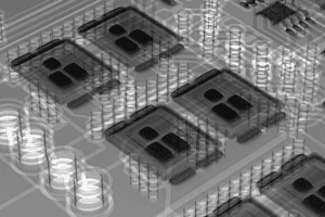
PCB Inspection Methods and Their Limitations
Inspection methods are the first line of defense in electronics manufacturing. Each method plays a role in catching defects before they leave the factory. Knowing both the strengths and the blind spots of these tools is what allows manufacturers to build reliable inspection strategies.
Manual Visual Inspection (MVI)

A technician looks at the board, sometimes with magnification or controlled lighting. A visual inspection works well for obvious defects such as solder bridges, scratches, or parts placed out of alignment.
The drawback is that human inspection is inconsistent. Fatigue sets in quickly, errors slip through, and complex boards with hidden joints are impossible to check this way. MVI is useful as a quick screen, but it cannot be scaled to cover modern assemblies.
Solder Paste Inspection (SPI)
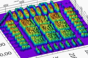
Source: Fulltronics Corporation LTD
Most defects in surface-mount assembly start with solder paste. SPI systems use 3D optical measurement to check paste height, volume, and alignment immediately after printing. Catching an offset or insufficient deposit here prevents downstream solder problems that would otherwise show up at reflow.
The limitation is scope. SPI only verifies paste, not component placement or solder joint quality. It requires regular calibration and process control, but when used correctly it saves significant time and rework.
Automated Optical Inspection (AOI)
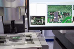
Source: Wevolver
AOI has become a standard checkpoint after placement and reflow. High-resolution 2D and 3D cameras compare each assembly to CAD data or a golden reference board. These systems excel at finding missing or misaligned parts, polarity errors, insufficient solder, and cosmetic defects.
Inline AOI adds speed to high-volume lines, while offline AOI is valuable for detailed checks or lower-volume runs.
What AOI cannot do is see through components. Joints under BGAs or other bottom-terminated packages remain hidden. Shadowing in dense layouts can also make detection less reliable.
X-Ray Inspection (AXI)
Source: Kuttig Electronic
Where AOI stops, X-ray inspection begins. AXI reveals the hidden world inside the board, from solder balls under BGAs to barrel fill in through-hole vias. With 2D, 2.5D, and full 3D CT options, manufacturers can examine voids, cracks, or misalignments that no optical system could catch.
The trade-off is cost and speed. X-ray machines are more expensive to purchase and maintain, and 3D imaging in particular adds cycle time. AXI is indispensable for advanced packages and dense multilayer boards, but it is not practical as the only method in a production environment.
Comparison of PCB Inspection Methods
| Method | What It Detects | Where It’s Useful | Limitations |
| Manual Visual Inspection (MVI) | Obvious surface defects: solder bridges, scratches, misaligned parts | Quick checks, small runs, visual confirmation | Inconsistent, operator fatigue, not scalable, cannot see hidden joints |
| Solder Paste Inspection (SPI) | Solder paste height, volume and alignment | Immediately after paste printing, preventive checkpoint | Only covers paste, not placement or solder joints, requires calibration |
| Automated Optical Inspection (AOI) | Missing or aligned parts, polarity errors, insufficient solder, cosmetic issues | Post-placement and post-reflow, inline or offline | Cannot see through packages, limited by shadowing in dense layouts |
| Automated X-Ray Inspection (AXI) | Hidden solder joints, voids, BGA balls, barrel fill in vias | Dense SMT assemblies, multilayer boards, advanced packaging | Higher cost, slower throughput than optical methods |
No single method is enough on its own, and relying on operators to bridge the gaps often creates delays. The next step is connecting these inspections into a smoother, more reliable process.
How Robotics Eliminates Inspection Bottlenecks and Human Error
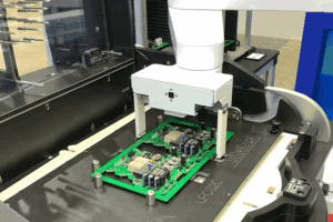
Even the best inspection systems create bottlenecks if people are still responsible for moving boards in and out of fixtures. Manual handling introduces variation, slows throughput, and limits how long a station can run without interruption. This is where robotics changes the equation.
Consistency
Collaborative robots can be assigned to the simple but repetitive task of loading and unloading boards at AOI, AXI, or other inspection stations. Every placement is consistent, reducing the chance of misaligned fixtures or dropped boards. That consistency improves the accuracy of the inspection itself and reduces false failures caused by poor handling.
Continuous Operations
Robots also allow inspection to run continuously. With automated loading, stations maintain predictable cycle times instead of pausing whenever operators are unavailable. This keeps throughput steady without depending on additional staff.
Workspace Density
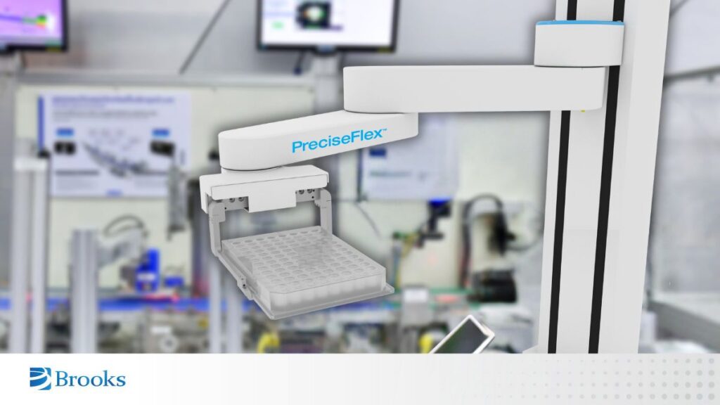
Another advantage is fit. Traditional industrial robots often require caged-off space that is not practical in a dense electronics line. Compact collaborative models, like PreciseFlex robots from Brooks Automation, are designed for tight footprints and can work safely alongside operators. This allows you to add automation without redesigning the entire test cell.
The benefits are straightforward:
- Higher throughput with less labor dependency
- Safer, more ergonomic workflows in high-mix cells
- Reduced downtime and scrap caused by handling errors
For a closer look at how these systems are implemented in practice, including cost considerations and case studies, download our PCB Automation Whitepaper.
Implementing Multi-Method Inspection Workflows
No single inspection method can cover every potential defect on a modern PCB. Visual checks are fast but limited. AOI excels at surface-level accuracy but cannot see under components. AXI penetrates hidden joints but adds cost and cycle time. Each method has strengths and weaknesses, which is why the most reliable strategies layer them together.
A typical workflow might look like this:
- SPI before reflow to verify solder paste volume and alignment
- AOI after placement to catch missing parts, misalignment, and solder issues
- AXI for BGAs and hidden joints where optical methods fall short
Many lines run AXI selectively, focusing on BGA or QFN areas where the risk of hidden defects is highest.
The value comes from how these stages connect. When data from SPI, AOI, and AXI is integrated, it improves traceability and helps process engineers correct root causes rather than just sorting out bad boards.
Automation ties these inspection stages together, keeping transitions consistent and feeding data directly into MES for closed-loop feedback.
PreciseFlex robots are designed with these workflows in mind.
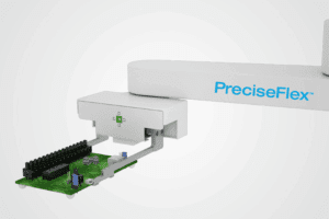
- Their compact form and vertical reach allow them to fit in crowded test cells.
- Built-in vision and dual grippers simplify fixture or magazine loading.
- Easy integration with MES helps manufacturers tie inspection directly to production data.
Inspection alone does not guarantee full coverage. That is why testing methods such as ICT, flying probe, boundary-scan, and functional tests are usually layered after inspection to verify electrical performance and complete the QA process. For a deeper look into those methods, see our PCB Testing article [LINK].
Future-Proofing Your Inspection Strategy
Inspection requirements continue to change as electronics become smaller, denser, and more critical to everyday life. Strategies that worked for larger boards or simpler assemblies are no longer enough.
To stay ahead, manufacturers are investing in tools and workflows that are 3D, connected, and automation-ready.
Miniaturization Driving 3D Inspection
Miniaturization is one of the strongest drivers of change. Boards now carry more components in less space, and packages such as BGAs and CSPs require imaging beyond what 2D AOI can provide. This is why 3D AOI and 3D CT X-ray are becoming standard. They allow precise measurement of solder joints, voids, and hidden interconnects that older systems can’t capture.
AI Improving Defect Classification
Machine learning models trained on production data improve defect classification, cut false calls, and stabilize first-pass yield. Instead of spending time reviewing borderline cases, engineers can focus on process improvements.
Connectivity and Industry 4.0 Integration
Connectivity is also reshaping inspection. New communication standards allow SPI, AOI, and AXI data to flow directly into MES and SPC systems, creating traceability and enabling predictive maintenance. This shift turns inspection from a quality checkpoint into a process control tool.
Automated inspection reduces labor dependence, improves yield, and scales capacity without expanding floor space. For manufacturers under pressure to deliver more with less, combining advanced imaging, connected data, and robotic handling is the most practical way to stay ahead.
Integrating Automation for Smarter PCB Inspection
Inspection methods only deliver their full value when they work together as part of a connected workflow. By handling transfers between stations, collaborative robots remove delays, reduce variation, and keep inspection running with consistent cycle times. The result is a process that delivers reliable coverage without adding labor or slowing production.
Brooks PreciseFlex robots are purpose-built for compact PCB test cells and high-mix inspection workflows. Their workspace-dense design and vertical reach make them easy to integrate, while built-in vision and dual grippers simplify board and fixture handling. The result is inspection that runs faster, more consistently, and more reliably.